How Do Circuit Boards Work?
(PCBs) form the foundation of virtually every electronic device we use. From smartphones to sophisticated medical equipment, these remarkably engineered boards are essential to modern electronics. But how exactly do these complex components function, and what makes them so vital to electronic devices? Read on to find out exactly how circuit boards work.
The Foundation of Modern Electronics
A standard PCB in its most basic form is a plastic board covered in fibreglass. Components are mounted on a non-conductive board and connected with small pathways, called traces. These traces allow the electrical components across the board to function by passing electricity through.
The Anatomy of a Circuit Board
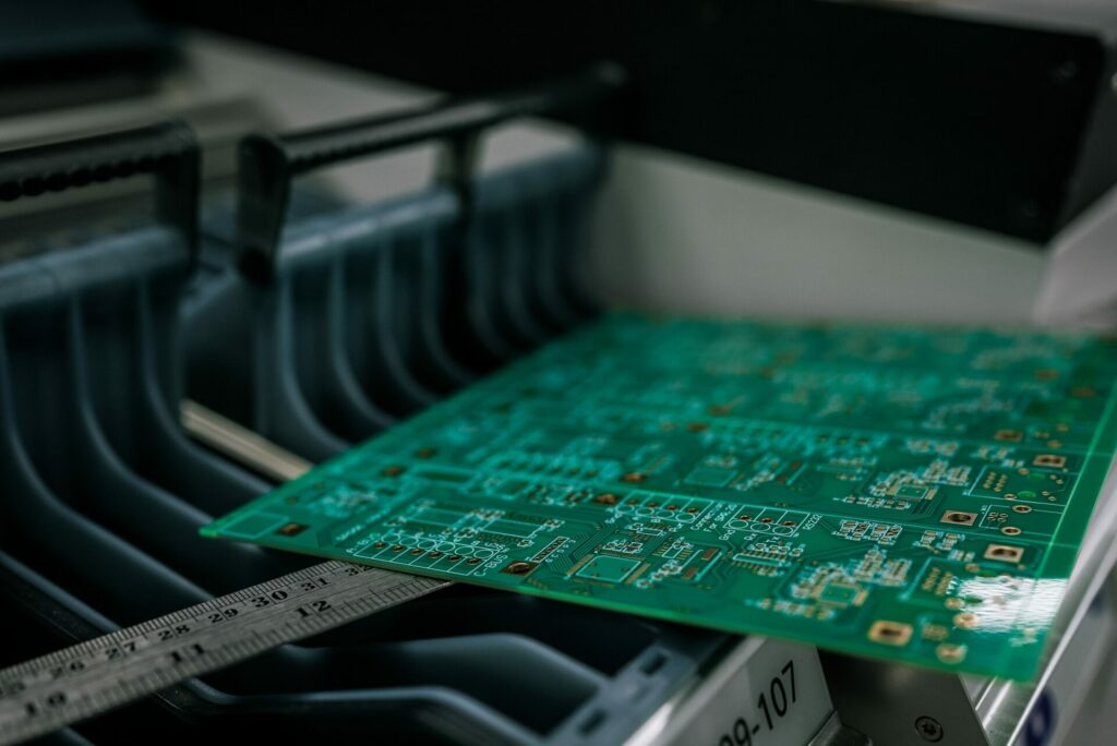
The foundation of every PCB starts with a base material, typically FR-4, a flame-resistant fiberglass-reinforced epoxy laminate. This base material offers excellent electrical insulation properties while maintaining strong mechanical stability. On top of this foundation, manufacturers apply a thin layer of copper, which will eventually form the conductive pathways essential for the board’s operation.
These conductive pathways, known as traces, are perhaps the most distinctive feature of any printed circuit board. Created through a precise etching process, copper traces act like miniature wires, forming predetermined routes for electrical signals to flow between components. Think of them as the roads in a city, connecting different locations (components) in carefully planned patterns.
Types of Printed Circuit Boards
Circuit boards come in several varieties, each suited to different applications and complexity levels:
Single-Sided PCBs
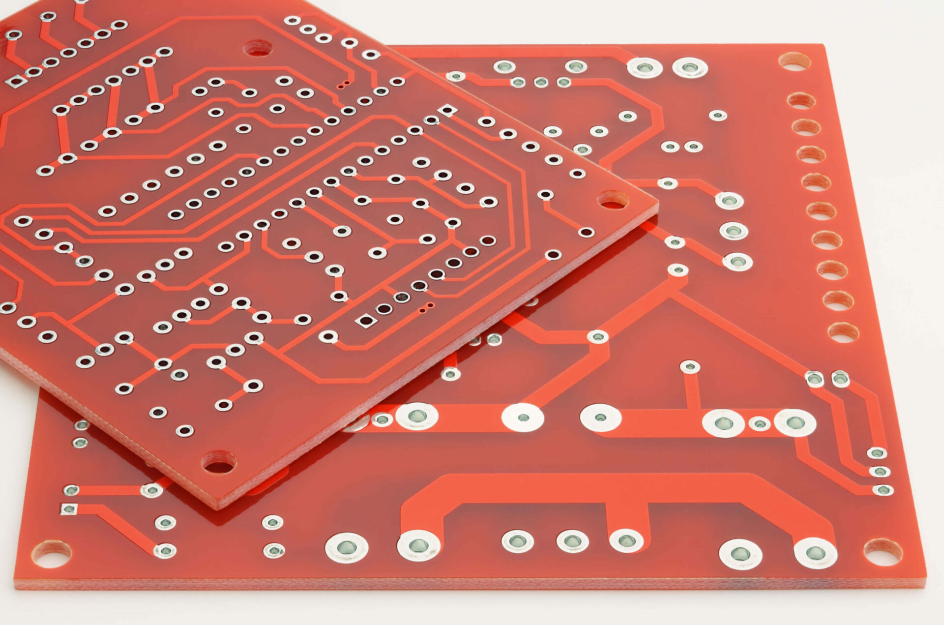
The most basic type includes copper traces on just one side of the board. Single-sided PCBs are often used in simpler electronic devices where straightforward circuit design is sufficient. These boards offer:
- Cost-effective manufacturing
- Easier design and production
- Ideal for high-volume, simple electronic products
- Common in calculators, simple LED displays, and basic power supply units
Double-Sided PCBs
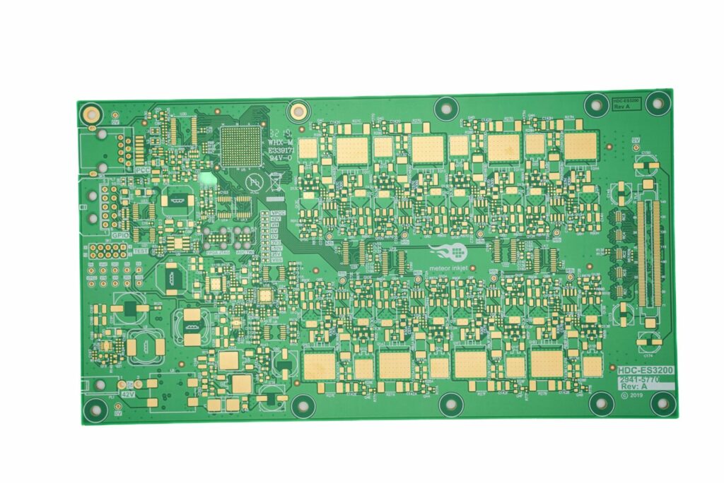
More sophisticated electronic products require double-sided PCBs, which feature conductive copper and components on both sides of the board. These boards employ special holes called ‘vias’ to connect circuits between layers. Double-sided PCBs offer:
- Increased circuit density
- More flexible routing options
- Better component placement optimization
- Enhanced design possibilities through the use of both surfaces
The PCB manufacturing process becomes more complex with double-sided boards, as components and route planning must consider both surfaces of the PCB. Special plated-through holes ensure reliable electrical connections between the two sides, allowing signals to pass seamlessly through the board.
Surface Finish Importance
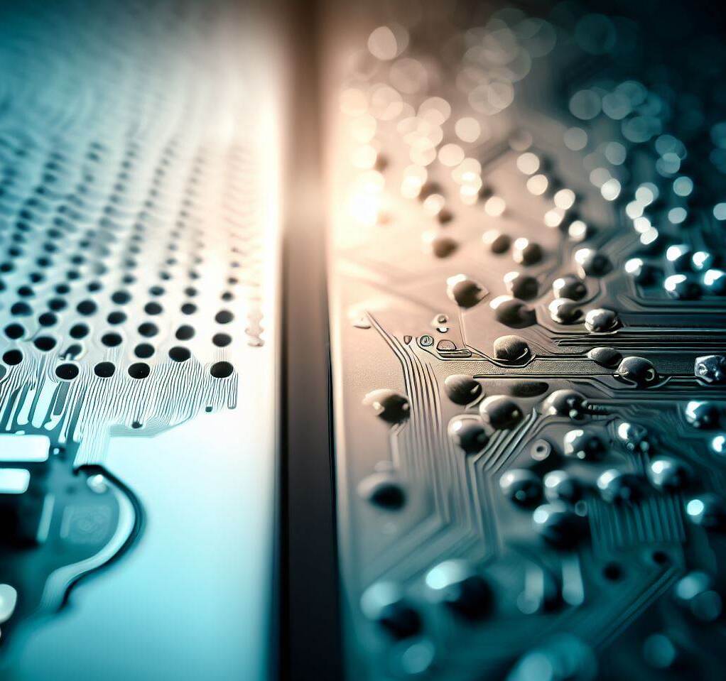
The surface finish of a PCB plays an important role in its functionality and longevity. Common finishes include:
- HASL (Hot Air Solder Leveling)
- ENIG (Electroless Nickel Immersion Gold)
- Immersion Tin
- Immersion Silver
Each finish offers different benefits for component soldering, environmental protection, and shelf life of the bare board. The choice of surface finish can significantly impact the assembly process and the final product’s reliability.
The Role of Copper in PCB Design
Copper’s role in PCB functionality cannot be overstated. This highly conductive metal forms:
- Signal traces for data transmission
- Power planes for voltage distribution
- Ground planes for electrical reference and shielding
- Thermal management paths
The thickness of copper layers, measured in ounces per square foot, is carefully specified based on current-carrying requirements and manufacturing constraints. Standard thicknesses range from 0.5oz to 3oz, with specialty applications using even thicker copper for high-power applications.
Essential Components of a Circuit Board
Understanding how circuit boards work requires a look into the electronic components that make modern devices possible. These components work together in harmony, each serving specific functions that contribute to the overall operation of the printed circuit board. Each component type must be carefully selected during the PCB design process to ensure optimal performance.
Active Components

Integrated Circuits (ICs)
Integrated circuits represent the pinnacle of electronic miniaturisation, packing incredible computing power into tiny packages. Often referred to as microchips, these sophisticated components contain entire circuits within a single component, sometimes incorporating millions of transistors, resistors, and other elements on a microscopic scale. ICs revolutionised electronic devices by making them smaller, more powerful, and more reliable.
Key types of ICs include:
- Microprocessors that serve as the ‘brain’ of computers and smart devices
- Memory chips that store both permanent and temporary data
- Signal processors that handle complex calculations and data manipulation
- Voltage regulators that maintain stable power supply
- Logic gates that perform fundamental computing operations
Transistors
Transistors are semiconductor devices that form the building blocks of modern electronics. These versatile components can amplify signals and act as switches, making them essential for both analog and digital circuits. In PCB design, transistors are crucial for controlling larger electrical signals with smaller ones, enabling efficient power management and signal processing.
Common transistor applications include:
- Signal amplification in audio and communication circuits
- Digital logic operations in computing devices
- Power control in motor drivers and LED displays
- Switching functions in digital circuits
- Voltage regulation in power supplies
Passive Components
Resistors
Resistors are fundamental components that control current flow through a circuit. Like a water valve in a plumbing system, resistors regulate the amount of electrical current that can pass through specific parts of the circuit. Their precise values are crucial for proper circuit operation and component protection.
Essential resistor functions:
- Current limiting to protect sensitive components
- Voltage division for signal scaling
- Heat generation for specific applications
- Pull-up or pull-down operations in digital circuits
- Biasing for transistors and other active components
Capacitors
Capacitors serve as temporary energy storage devices in electronic circuits. These components can quickly store and release electrical charge, making them invaluable for power management and signal processing. Their ability to block DC while allowing AC signals to pass makes them versatile circuit elements.
Key capacitor applications:
- Power supply smoothing to reduce voltage ripple
- Signal coupling and decoupling between circuit stages
- Timing circuits for oscillators and delays
- Frequency filtering in audio and RF circuits
- Noise suppression in sensitive electronics
Inductors
Inductors are components that store energy in magnetic fields when current flows through them. They play a crucial role in filtering and power conversion circuits. Their ability to resist changes in current flow makes them essential for many applications where stable current is needed.
Critical inductor uses:
- Signal filtering in radio frequency circuits
- Noise reduction in power supplies
- Voltage conversion in switch-mode power supplies
- Energy storage in power circuits
- EMI suppression for regulatory compliance
Manufacturing, Assembly, and Applications
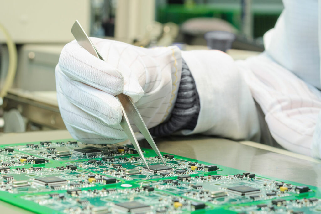
The journey from design to finished printed circuit board involves multiple sophisticated processes. Understanding how circuit boards work requires knowledge of not just the components, but how they come together in manufacturing to create functional electronic devices.
PCB Manufacturing Process
Design and Layout
Every circuit board begins with careful planning and design. Engineers use specialised PCB design software to create detailed schematics and board layouts. This crucial first step determines the success of the final product and requires consideration of numerous factors including signal integrity, power distribution, and thermal management.
Key design considerations include:
- Component placement and spacing
- Copper trace width and spacing
- Power and ground plane design
- Thermal considerations
- Signal integrity requirements
- Manufacturing tolerances
Base Material Preparation
The foundation of every PCB starts with the careful preparation of the base material, typically FR-4 fiberglass. This process ensures the structural integrity and electrical properties of the final board.
Essential base material properties:
- Flame retardant characteristics
- Mechanical strength
- Dimensional stability
- Electrical insulation
- Thermal resistance
- Chemical resistance
Copper Processing
The application and processing of copper layers is a precise operation that creates the conductive pathways essential for circuit function. This process involves multiple steps to ensure reliable electrical connections.
Critical copper processing steps:
- Cleaning and preparation
- Photoresist application
- Pattern exposure
- Chemical etching
- Copper thickness verification
- Surface finishing
Assembly Techniques
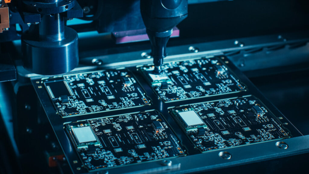
Surface Mount Technology (SMT)
Modern PCB assembly primarily uses SMT, where components are mounted directly onto the surface of the board. This technology enables higher component density and more efficient manufacturing.
SMT process highlights:
- Solder paste application through stenciling
- Automated component placement
- Reflow soldering in controlled ovens
- Inspection and quality control
- Higher production speeds
- Reduced assembly costs
Through-Hole Assembly
Though less common in modern electronics, through-hole assembly remains important for certain components that require stronger mechanical connections or higher power handling.
Through-hole advantages:
- Stronger mechanical bonds
- Better thermal management
- Easier manual rework
- Higher reliability in harsh environments
- Suitable for high-power components
Testing and Quality Assurance
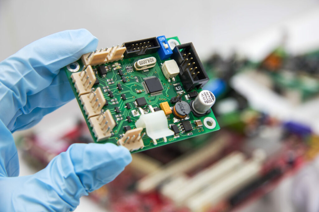
Electrical Testing
Comprehensive testing ensures each board functions as intended. Multiple testing methods are employed to verify circuit integrity and component functionality.
Testing methods include:
- Automated optical inspection (AOI)
- In-circuit testing (ICT)
- Functional testing
- Flying probe testing
- X-ray inspection
- Burn-in testing
Environmental Testing
Many PCBs must undergo environmental testing to ensure reliability in their intended operating conditions.
Environmental factors tested:
- Temperature extremes
- Humidity resistance
- Vibration tolerance
- Shock resistance
- Chemical exposure
- EMI compliance
Our exploration of how circuit boards work demonstrates the complexity and precision required in modern electronics manufacturing. From initial design through final testing, each step contributes to creating reliable, high-performance electronic devices that power our modern world.
Looking to manufacture your own PCBs? Contact ABL Circuits to discuss your requirements and how we can help bring your electronic designs to life.
Frequently Asked Questions About Circuit Boards
Q: What’s the difference between “rigid” and “flexible” PCBs, and when would you use each?
A: Rigid PCBs are the traditional solid circuit boards found in most electronics, while flexible PCBs are made with bendable materials that allow them to fit into curved spaces or move during operation. Flexible PCBs are commonly used in cameras, mobile phones, and medical devices where space is tight or movement is required. Rigid PCBs are typically more cost-effective and are used in most standard electronic devices.
Q: How long does a printed circuit board typically last?
A: Under normal operating conditions, a well-manufactured PCB can last 20+ years. However, lifespan depends on various factors including environmental conditions (temperature, humidity, vibration), quality of components, usage patterns, and manufacturing quality. Regular maintenance and proper operating conditions can significantly extend a PCB’s life.
Q: Can a damaged circuit board be repaired?
A: Yes, many types of PCB damage can be repaired by skilled technicians. Common repairs include replacing damaged components, repairing broken traces, and fixing lifted pads. However, some damage, particularly to multilayer boards or involving burnt internal layers, may be irreparable. In these cases, board replacement is necessary.
Q: What’s the smallest size a PCB can be manufactured?
A: Modern PCB manufacturing can produce boards as small as 0.4mm in thickness with traces as narrow as 0.075mm. However, practical limitations often come from component size and handling requirements rather than manufacturing capabilities. The minimum viable size depends on your specific components and design requirements.
Q: How do manufacturers ensure PCBs are environmentally friendly?
A: PCB manufacturers implement various eco-friendly practices including lead-free solder, RoHS-compliant components, recycling of waste materials, and use of environmentally sustainable cleaning agents. Many also offer options for biodegradable board materials and work to minimize energy consumption during production.
Q: What determines the thickness of a printed circuit board?
A: PCB thickness is determined by several factors including the number of layers, base material thickness, copper weight, and required rigidity for the application. Standard thicknesses range from 0.8mm to 1.6mm, but specialty applications can require boards as thin as 0.4mm or as thick as 3.2mm. The choice depends on mechanical requirements, component types, and intended use.
If you’d like to find out more about how circuit boards work, what is a circuit board made of, or how ABL Circuits can help you with your project, get in touch for more information.

Fast
You will benefit from the fastest leadtimes in the UK. Your ABL Circuits PCB’s will be delivered within 5 working days as standard.

Friendly
Your order will be dealt with promptly by a friendly and conscientious team, committed to providing a high level of service.

Exceptional
You will also benefit from our exceptional 8 hour same day express service for your urgent prototypes.
Experienced
The knowledge gained from 40 years of experience eliminates your risk in dealing with ABL Circuits.
Dependable
Your deadlines are critical to you and us, that’s why we guarantee you will receive your boards on time, every time in perfect condition.
